当前位置:首页 > 商业/管理/HR > 质量控制/管理 > wafer introduction
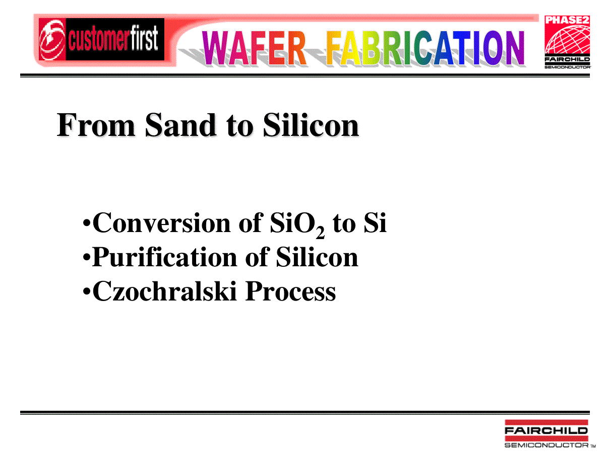
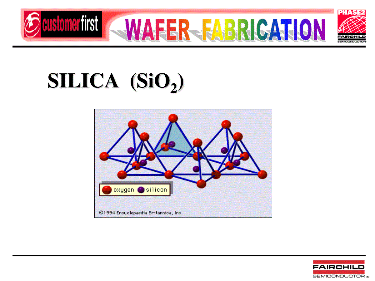
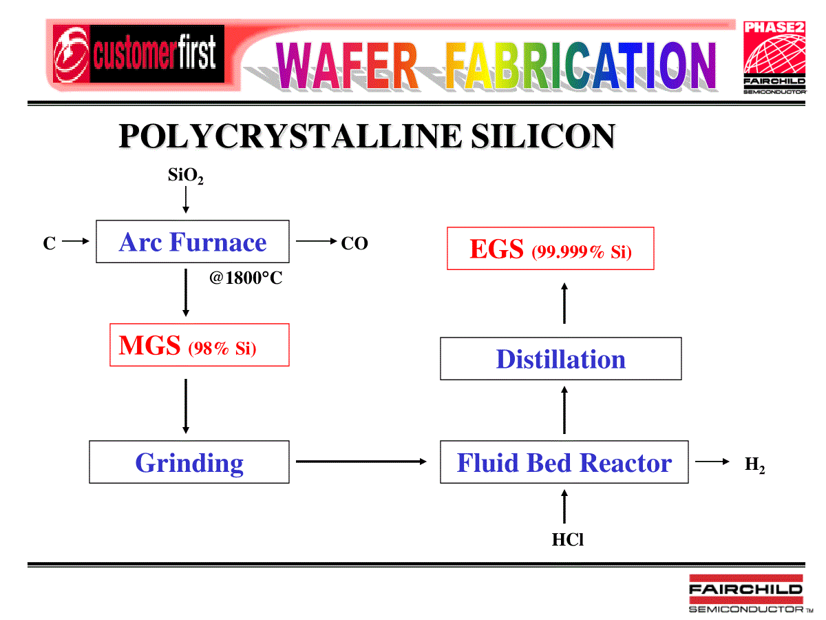
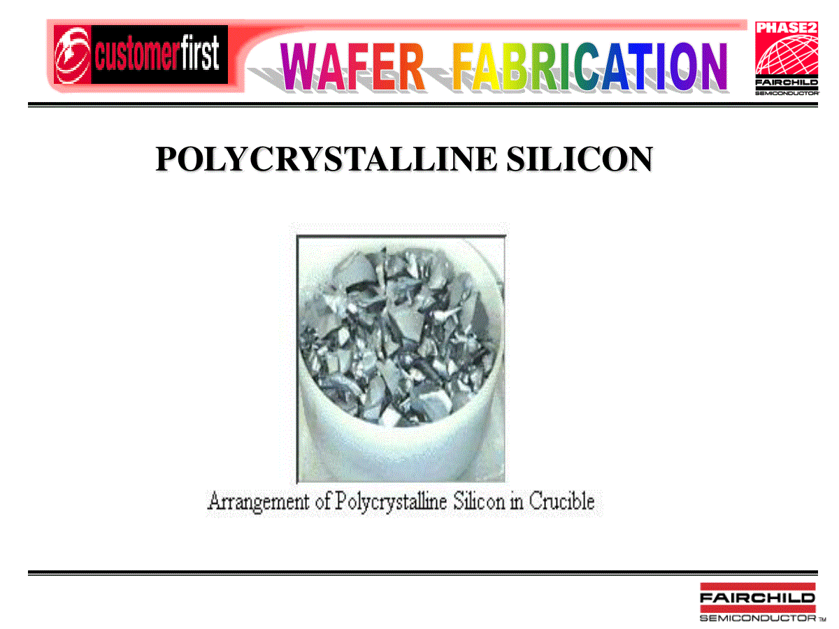
Page1Page2•ConversionofSiO2toSi•PurificationofSilicon•CzochralskiProcessFromSandtoSiliconPage3SILICA(SiO2)Page4POLYCRYSTALLINESILICONArcFurnaceSiO2CMGS(98%Si)GrindingFluidBedReactorDistillationCO@1800CEGS(99.999%Si)HClH2Page5POLYCRYSTALLINESILICONPage6POLYCRYSTALLINESILICONTOSINGLE-CRYSTALSILICONPage7SingleCrystalSiliconCzochralski(CZ)MethodPage8Page9SingleCrystalSiliconCzochralski(CZ)MethodPage10SingleCrystalSiliconIngotPage11SingleCrystalSiliconIngotPage12-WaferShapingSlicingLappingEtching-Polishing-CleaningandInspectionWaferProductionPage13SLICINGPage14Page15LAPPING•Removalofsurfaceroughnessfromsawcutsandprocessdamage•UsesamixtureofAl2O3powderandH2OPage16ETCHING•Removalofsurfacedamage/microcracksinducedbyAl2O3abrasiveduringlapping•EtchingisdoneusingamixtureofHNO3andglacialaceticacidsolutionPage17CHEMICAL-MECHANICALPOLISHING(CMP)SilicapowderisdissolvedinDIwaterandcontrolledatapH10-11withNaOH,andthenfedontothewaferswhicharesimultaneouslybuffedbyapolishingpadofartificialleatherThisremovesanyremainingsurfaceroughness.Combinedeffectofmechanicalandchemicalapproachensuresthatthereisnoadditionaldamageduringtheprocess.Page18WAFERCLEANA3-stepprocessusedtocleanwafers1.SC-1solutionNH3,H2O2andH2Oremovesorganicimpurities2.HFsolutionremovesnaturaloxidesandmetalimpurities3.SC-2HClandH2O2growaclean,newnaturaloxideonthesurfaceofthewaferPage19Layering-growordepositthinlayeronwafersurface-Oxidation,CVD,Evaporation,SputteringPatterning-selectiveremovaloflayersonthewafer-photolithography,etchingDoping-changeconductivitytypeofselectedportionofwafer-thermaldiffusion,ionimplantationThreeBasicStepsinWaferFabricationPage20LayeringOriginalLayerGrownLayerPage21PatterningOriginalLayerGrownLayerStepusuallyinvolved:-photoresistapplication-Patterndefinition(UVlightexposure)-Development-etchingPage22DopingOriginalLayerDopantPage23DopingOriginalLayerDiffusedLayerCommonDopants:-Ntype(Phosphorous)-Ptype(Boron)Page24Page25Page26Page27Page28Page29Page30Page31Page32Page33Page34Page35Page36Page37Page38Page39Page40Page41Page42Page43Page44Page45Page46Page47AnInitialOxideisgrownoverthestartingmaterial(composedofepi&substrate)DrawnbyEdgarAncajas01/25/2001InitialOxidePhosphorusEPI,7MicronsThick,0.66Ohms/CmArsenicSubstrate127InitialOxide40(8250+/-600A950C,Wetw/DCE130ScribeCoat(ResistCoatforLaserScribe)135Scribe(LaserScribeLot#andWafer#forIdentification145ResistClean1(RemovesScribePhotoresist)165CleanInspect(VerifyallResisthasbeenremoved)PLANARDMOSWAFERFABFLOWPage48Photoresistisapplied&etchedtodefinetheFieldOxide.3451.0Photo(DefineActiveArea)3461.0Descum(55W,23s,TegalPlasmaDescum)PLANARDMOSWAFERFABFLOWPage49PLANARDMOSPROCESSFLOWTheInitialOxideisetchedtocreatethoseActiveAreas.403SinkEtch44(13:2BOE,10KATarget~12min)4051.0EtchInspect(VerifyallOxideisremoved)Page50AClean(Gate)Oxideisthengrown.ThisistheGateOxide.ThePhotoresistisstripped.413WetClean(H2S04/H202,8:13X10m)414CleanInspect(Verifyallresisthasbeenremoved)2576MosClean1(Piranha-200:1HF-SC1-SC2-SRD)2660GateOxide45(800+/-75A900C,wetw/DCE–3.8DMOS-A,CFlowsonly2670GateOxide46(800+/-40A900C,wetw/DCE–3.8DMOS-BFlowsonlyPLANARDMOSWAFERFABFLOWPage51PolyprovidestheGateoftheDMOS.3005PolyDeposition30(5500+/-500A,630C(within4hoursofGateOx)3050EtchCoat(CoatfrontsideforbacksideEtch-12-12.3KAHunt504)3060BackEtch24(NF3Plasma,1Torr,52.5W,45sFixed)3102SinkEtch34(2.5min13:2BOE–ToSHEET3103BacksideWetClean(H2SO4/H2O2,8:13X10m3104CleanInspect(Verifyallresisthasbeenremoved)3107MosClean1(Piranha-200:1HF-SC1-SC2-SRD)3125POCL30(16mSoakat950CPOCL3V/I=2.2+/-.20)3190Deglaze1(1m10:1HF+10mPiranhaPLANARDMOSWAFERFABFLOWPage52PolyMaskdefinesthegateofthedeviceNote:DetailedPhotoandResiststripisnotshowntosimplifythings.33506.0Photo(PolydefinedCD)PLANARDMOSWAFERFABFLOWPage53UnwantedPolyisetched.3387PolyEtch14(PolyEtch–SF6/C12/He+C12/HeEP+C12/HeOE34836.0EtchInspect(VerifyallPolyisremovedandToxiscorrect)PLANARDMOSWAFERFABFLOWPage54TheGateisnowdefined.DeviceisreadyfortheP-WellImplant.34896.0Strip(Plasma)(PlasmaStrip–CFPolymerRemoval)35046.0WetClean(H2SO4/H202,8:13X10m35096.0FI&CD(VerifyCD’sandcompletePhotoresistremoval,CD:7.0um)PLANARDMOSWAFERFABFLOWPage55P-Wellregionsaredefinedhere.FirstwiththeP-WellImplantandthentheDrive4365P-Well40Implant(5.3E13,B11@70KeV–3.8DMOS-A,BFlowsonly4369P-Well43Implant(2.8E13,B11@70KeV–3.8DMOS-CFlowsonly4615MOSClean1(Piranha-100:1HF-SC1-SC2-SRD)4625P-Drive40(1100C,8hours,220+/-25A,VeryLow02)PLANARDMOSWAFERFABFLOWPage56P+40Implant,5.0E15,B11@60KeVDefiningtheP+HeavyBodyregion46407.9Photo(DefinesmallopeningsinPhotoresistforP+Imp–CD:3.6um)4675DeepUVC(Flash3s@120CCure80s@230C)4683P+40Implant(5.0E15,B11@60Kev)PLANARDMOSWAFERFABFLOWPage57Photoresiststrip46877.9Strip(PlasmaStripGas01recipe)46937.9WetClean(H2S04/H202,8:13X10m)4695CleanInspect(Verifyallresisthasbeenremoved)PLANARDMOSWAFERFABFLOWPage58P+Drive4760MosClean1(Piranha-200:1HF-SC1-SC2-SRD-3.8DMOS-A,Bonly)4761MosClean1(Piranha-200:1HF-SC1-SC2-SRD-3.8DMOS-Conly)4770P+Drive40(1100C,1hour,110+/-25A,VerylowO2-3.8DMOS-A,Bonly)4771P+Drive41(1100C,1h
 三七文档所有资源均是用户自行上传分享,仅供网友学习交流,未经上传用户书面授权,请勿作他用。
 扫描二维码
扫描二维码


 petty131
本文标题:wafer introduction
链接地址:https://www.777doc.com/doc-4467427 .html